2 - PCB Assembly

Tony
Site Admin
Posts: 948
Joined: Tue Jul 24, 2012 8:05 pm

Re: 2 - PCB Assembly

Post by Tony »

Remove the wire offcuts from the 3v9 zener and attach them to either side of one of the HV capacitors. I'd recommend waiting a few minutes after the first test before doing this as they may still be charged up.

Image

Repeat the test with the meter now set on a 200V+ voltage range, the reading this time should stabilise around 160-170V.

If everything worked OK disconned the coil wires so you can work on the PCB again - it's time to fit the PIC and nixie sockets.
Tony
Site Admin
Posts: 948
Joined: Tue Jul 24, 2012 8:05 pm

Re: 2 - PCB Assembly

Post by Tony »

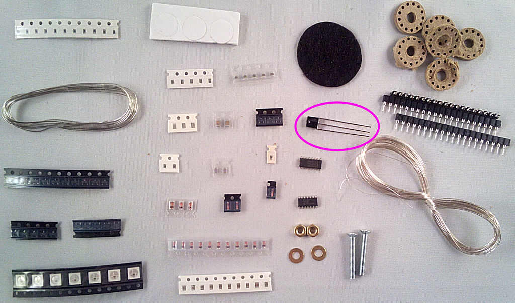
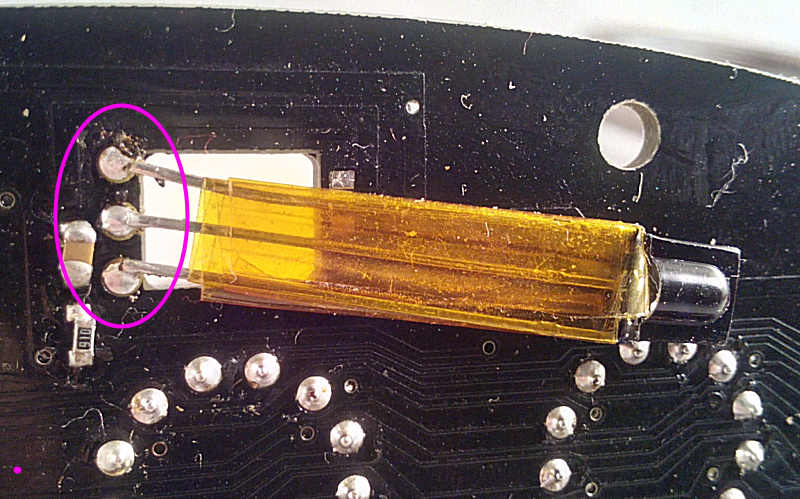
Wrap the legs of the 3-legged IR receiver in insulation tape to prevent them shorting against anything on the PCB and solder it to these 3 pads with the domed side of the sensor facing up. This puts it in a better position for IR reception than the original PCB cutout, needed due to a design change on the base lid.

Image

Image
Tony
Site Admin
Posts: 948
Joined: Tue Jul 24, 2012 8:05 pm

Re: 2 - PCB Assembly

Post by Tony »

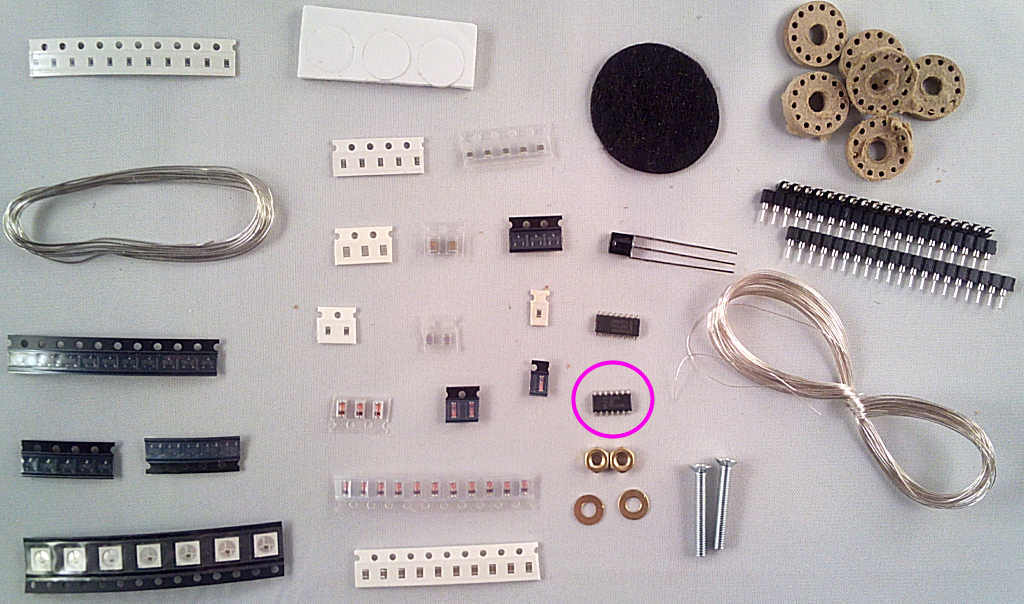
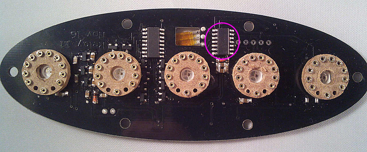
The last electronic component before the nixie sockets - the PIC. The pin 1 marker dot faces DOWN towards the zener diode this time.

Image

Image
Tony
Site Admin
Posts: 948
Joined: Tue Jul 24, 2012 8:05 pm

Re: 2 - PCB Assembly

Post by Tony »

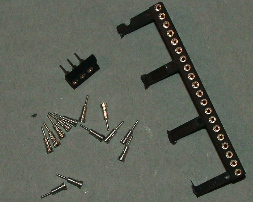
Time to assemble the sockets. Using wirecutters or pliers carefully break the turned pin sockets out of the plastic housing:

Image

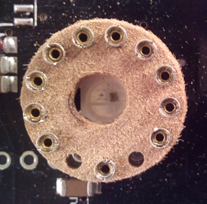
Push the pins into the socket former - Use this pattern of pins for IN-14 nixies:

Image

For IN-8-2 tubes move the anode (at the bottom, 6 o'clock position) to the empty hole on the left.
The decimal points aren't used on any tube so cut this lead short. For IN-8-2 tubes, you'll need to bring the k1 pin across to the unused socket under the DP pin.

You'll need 5 of these made up, either 5x IN-14 tubes or 4x IN-8-2 and 1x IN-14.

Solder them into the PCB - the pins will just clear the holes with the former resting on the LED. If you're using IN-8-2 tubes the single IN-14 socket is used in the centre for the colon IN-19 tube.
Tony
Site Admin
Posts: 948
Joined: Tue Jul 24, 2012 8:05 pm

Re: 2 - PCB Assembly

Post by Tony »

Now fit the nixies - these instructions cover the IN-14 tubes and assume they were supplied with the kit. The sockets are considered to be V1-V5 from right to left:

Take the 2x nixies (1x IN-19B and 1x IN-14) out of their packing and straighten the wires, spreading them out slightly to match the diameter of the socket. If any are uneven or slightly longer than the others you can trim them a little to match - but not too much. They're already cut to approximately the right length before being packed.

Note the white ceramic paint on one of the wires inside the tube, at the back. This is the anode and must face directly to the back of the PCB (away from the ICs) when fitted. Ignore the short wire stub at the front of the IN-19, it's a second anode which isn't counted as a real pin and should be removed. The IN-14 decimal point pins have been removed as they would cause problems (one of the PCB DP pins is connected to the anode).

Take the numerical nixie tube from the pack of 2:

Starting with that anode wire, fit it into the topmost hole of the socket in the V5 position, follwed by one wire in sequence into each hole. Make sure the white-topped anode lead is still in the correct place, it's easy to slip one place whilst fighting (or fitting) it in. Push it down carefully into the socket pins. (You can fit them in any order you're happy with, I usually work from right to left).

Take the 3x IN-14 nixies out of their packing and straighten the wires as before. Fit one into the socket for V4, next to V5 and fit the IN-19B tube into the V3 socket, follwed by the remaining 2x IN-14 nixies in V2 and V1. You should now have 2 pairs of numerical tubes separated by a symbol tube in the centre.

Once you're certain they're in the right places and are vertically aligned you may wish to solder 2-3 of the wires into the socket pins to prevent them being dislodged.
Tony
Site Admin
Posts: 948
Joined: Tue Jul 24, 2012 8:05 pm

Re: 2 - PCB Assembly

Post by Tony »

Or for IN-8-2 nixies (copied from our Coppertop but the method is the same)

Start with the pack of 2x nixies (1x IN-19B and 1x IN-8-2), take them out of their packing and straighten the wires, spreading them out slightly to match the diameter of the socket. If any are uneven or slightly longer than the others you can trim them a little to match.

Note the white ceramic paint on one of the wires inside the IN19, at the back. This is the anode and must face directly to the back of the PCB when fitted. Ignore the short wire stub at the front of the IN-19, it's a second anode which isn't counted as a real pin and can be removed if preferred.
The same 'anode' lead is missing from the IN-8-2 nixies though it faces the same way - so the gap in the pins is positioned over the '12 o'clock' socket pin, leaving it unused.

Take the numerical nixie tube from the pack of 2:

Starting with that gap where the anode wire would have been, position it over the topmost hole of the socket in the V5 position then push one wire in sequence into each hole. Make sure the missing lead 'gap' is still in the correct place, it's easy to slip one place whilst fighting (or fitting) it in. Push it down carefully into the socket pins. (You can fit them in any order you're happy with, I usually work from right to left).

Take the 3x IN-8-2 nixies out of their packing and straighten the wires as before. Remove the decimal point pin (pin 8) and bend k1 (pin1) so it takes its' place - do this for all 4 tubes. Fit one into the socket for V4, next to V5 and fit the IN-19B(V) tube into the V3 socket, followed by the remaining 2x IN-8-2 nixies in V2 and V1. You should now have 2 pairs of numerical tubes separated by a symbol tube in the centre.

Once you're certain they're in the right places and are vertically aligned you may wish to solder 2-3 of the wires into the socket pins to prevent them being dislodged.
Tony
Site Admin
Posts: 948
Joined: Tue Jul 24, 2012 8:05 pm

Re: 2 - PCB Assembly

Post by Tony »

Now reconnect the coil and test the complete assembly again. The nixies should light and display 00+00 with the coil about 1" from the base coil. Don't go any closer than that as it can cause overvoltage/current damage as the zener diodes may be overloaded.

Position the IR receiver si it can 'see' light from the base LEDs - the centre colon should now change from + to - every second and the nixie LEDs will change to blue. If the GPS mouse is set up and working, it should now display the time as received from the GPS module.

Disconnect the coil again and move onto the Case assembly instructions - it's done.
Zedsquared
Posts: 11
Joined: Tue Nov 07, 2017 9:56 pm

Re: 2 - PCB Assembly

Post by Zedsquared »

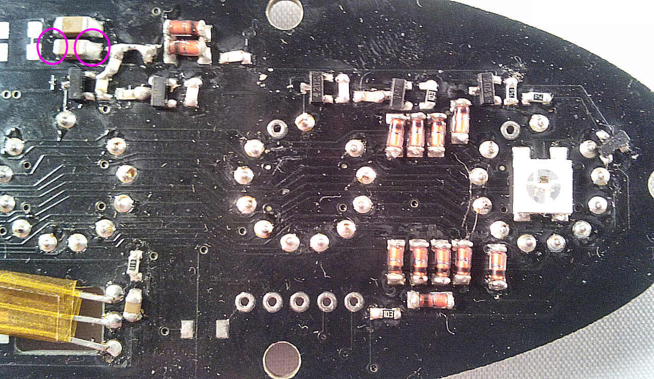
Tony wrote:Now a modification before going any further. There's a track connecting the HV capactiros to the main HV rail running between the MMBTA92 transistors here:

It's under the resistor in the picture but you can see where the PCB has been cut. Cut through this track as it's now connected to the HV supply by that resistor.
I'm afraid that what with the black solder resist, rather hairy PCB and shiny photo I can't positively identify the track you're referring to ... any chance of a picture of just the cut without any components obscuring it?

While I'm on ...I found that the diodes were best dealt with by generously tinning one end while they were held in heatsink tweezers to aid tacking them to the board.

Cheers,
Robin.
Tony
Site Admin
Posts: 948
Joined: Tue Jul 24, 2012 8:05 pm

Re: 2 - PCB Assembly

Post by Tony »

Check the 'PCB assembly help' thread for the correct track to cut.
Zedsquared
Posts: 11
Joined: Tue Nov 07, 2017 9:56 pm

Re: 2 - PCB Assembly

Post by Zedsquared »

Tony wrote:This should help:

Image
Yep, much clearer, thanks... Might I suggest an edit to the original text... The HV rail seems to run along *above* the transistors and I was taking "between" to mean "through the middle of" and not "shared amongst" so I was confused as the track that runs through the middle of the transistors isn't isolated by any cuts in the area highlighted.

Cheers,
Robin.
Locked