Page 2 of 3
Re: PCB assembly
Posted: Sun Apr 19, 2015 5:19 pm
by Tony
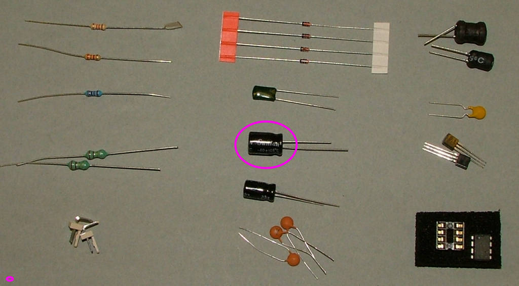
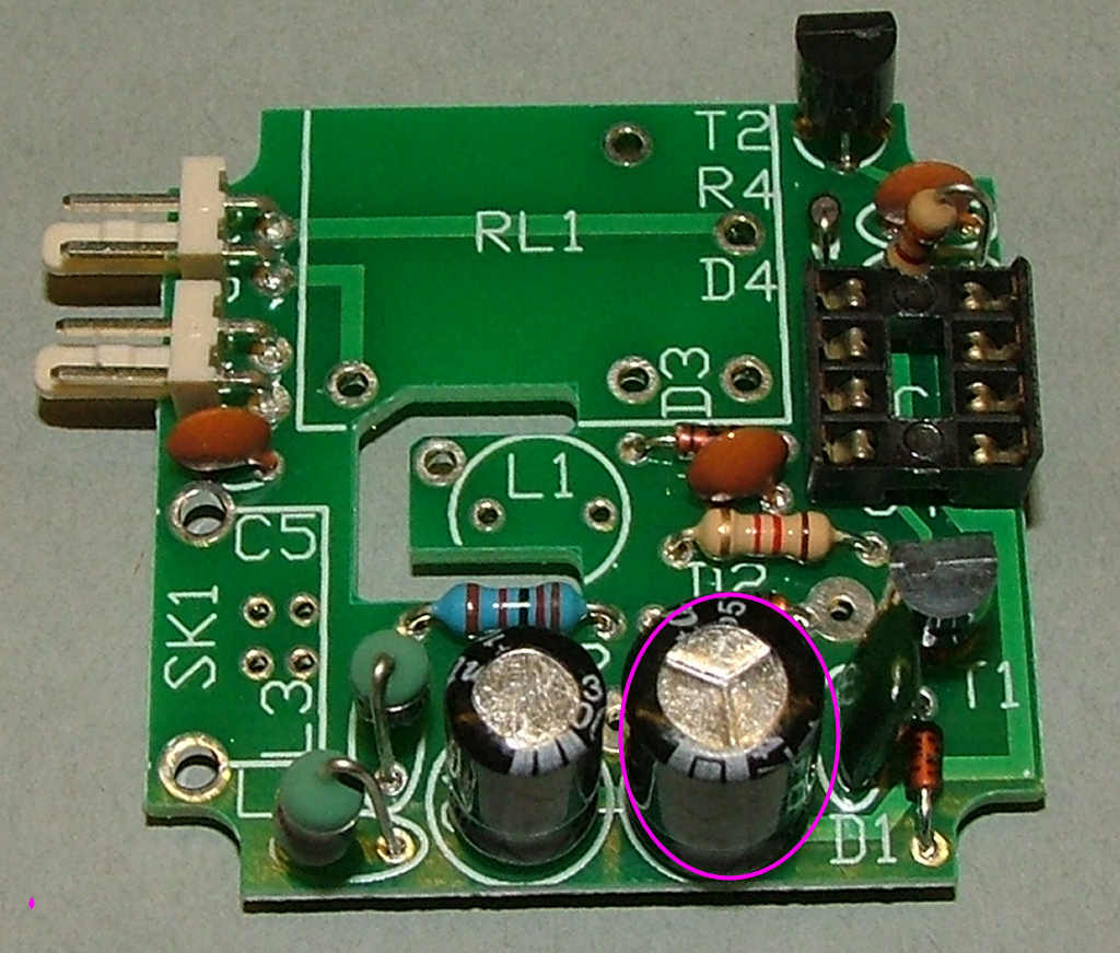
Next are the electrolytic capacitors. Fit the 470uF or 330uF smoothing capacitor into the C2 space, making sure the negative stripe faces the edge of the board:


Re: PCB assembly
Posted: Sun Apr 19, 2015 5:20 pm
by Tony
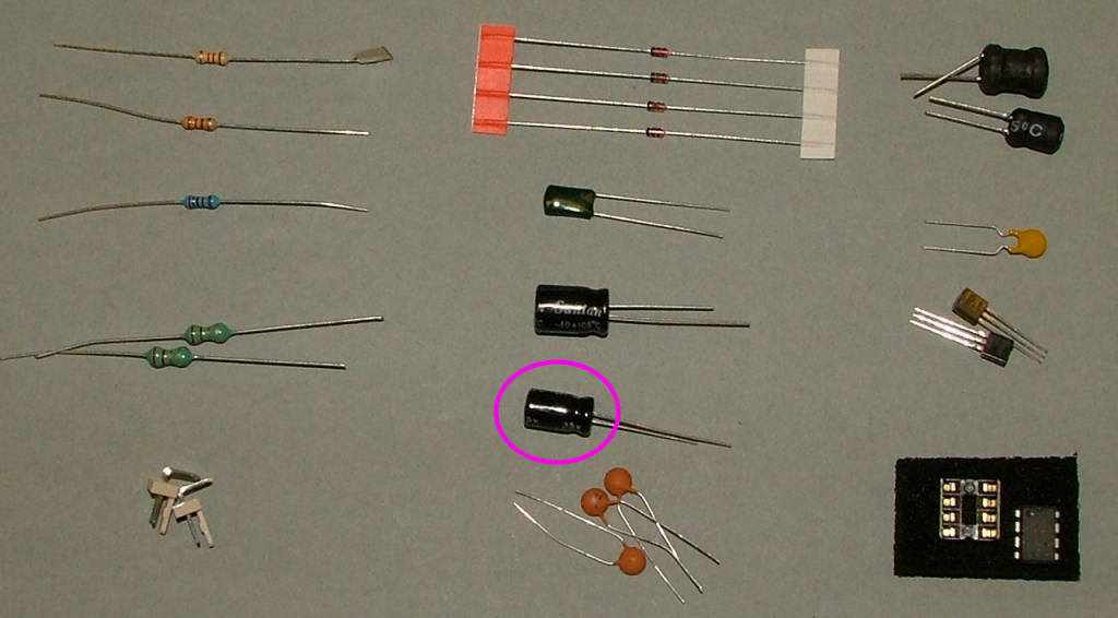
Followed by the 100uF or 220uF 25V. This one stores the power used to switch the relay contacts and is marked C1, making sure the negative stripe faces the edge of the board:


Re: PCB assembly
Posted: Sun Apr 19, 2015 5:23 pm
by Tony
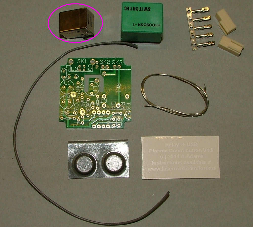
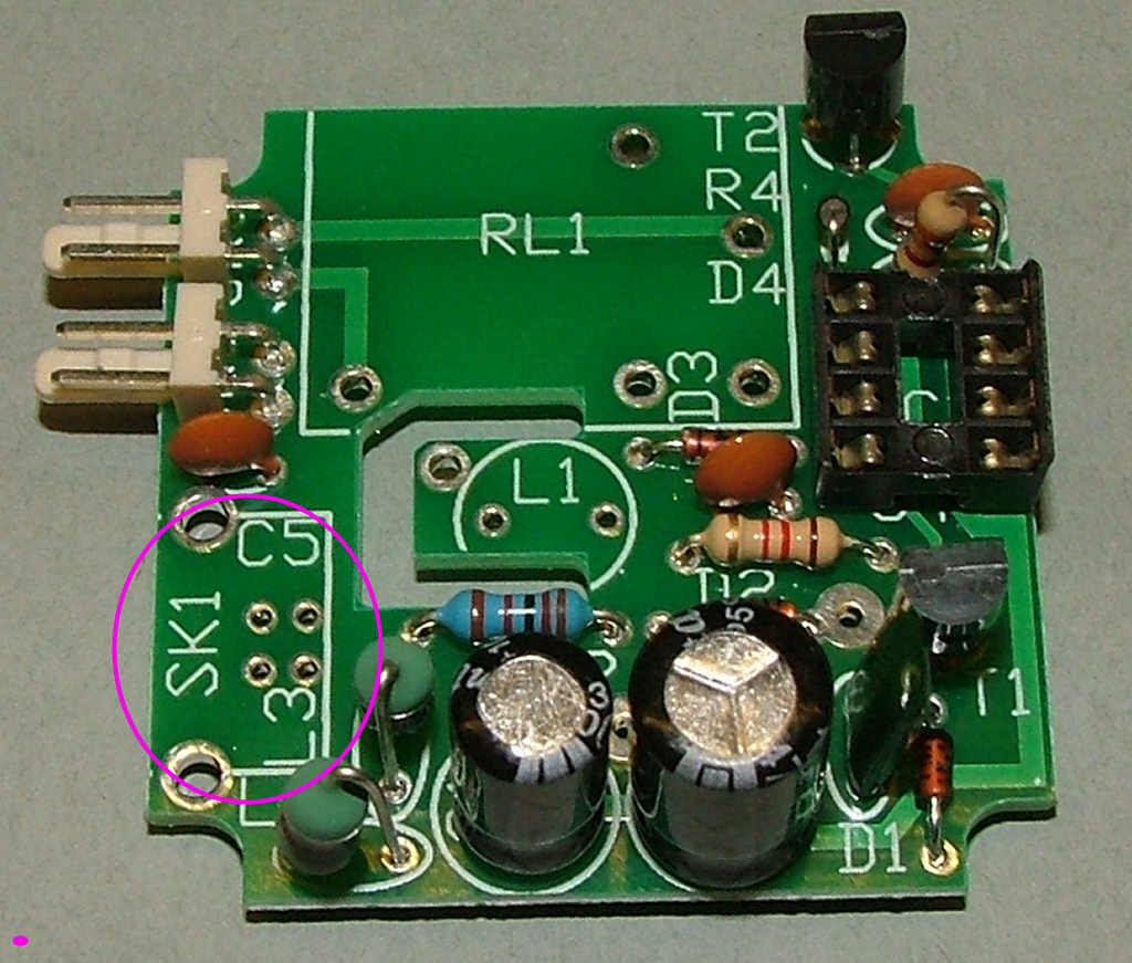
The last part for now is the USB socket, fit that in the SK1 holes:


Re: PCB assembly
Posted: Sun Apr 19, 2015 5:30 pm
by Tony
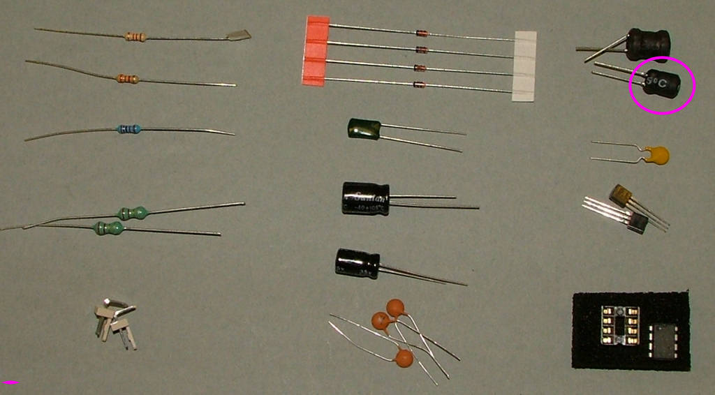
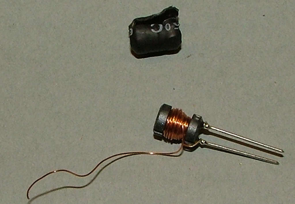
The next job is to make what will be used as the high voltage transformer - this is made from a 10mH inductor with a new primary winding added over the original coil. Take the 100uH coil (the smaller of the two radial inductors, if you have received two small inductors then it's the one with 2 short legs) and carefully remove the insulation covering it.
The only purpose of this part is to donate the wire to wind the primary.


Re: PCB assembly
Posted: Sun Apr 19, 2015 5:33 pm
by Tony
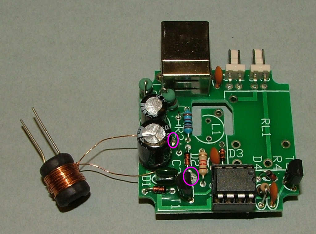
Carefully wind 27-28 turns around the larger coil - or the one with a long and a short leg if you received two small coils - as shown, leaving tails of about 1 1/2". Don't remove the insulation from that coil, just wind the wire over the top of it. You'll probably need all the wire from the first choke for this. Wind as evenly and neatly as possible and avoid leaving gaps or loose wire.
Tin the ends of these, the insulation should burn off using a soldering iron without needing to scrape it away.

Re: PCB assembly
Posted: Sun Apr 19, 2015 5:36 pm
by Tony
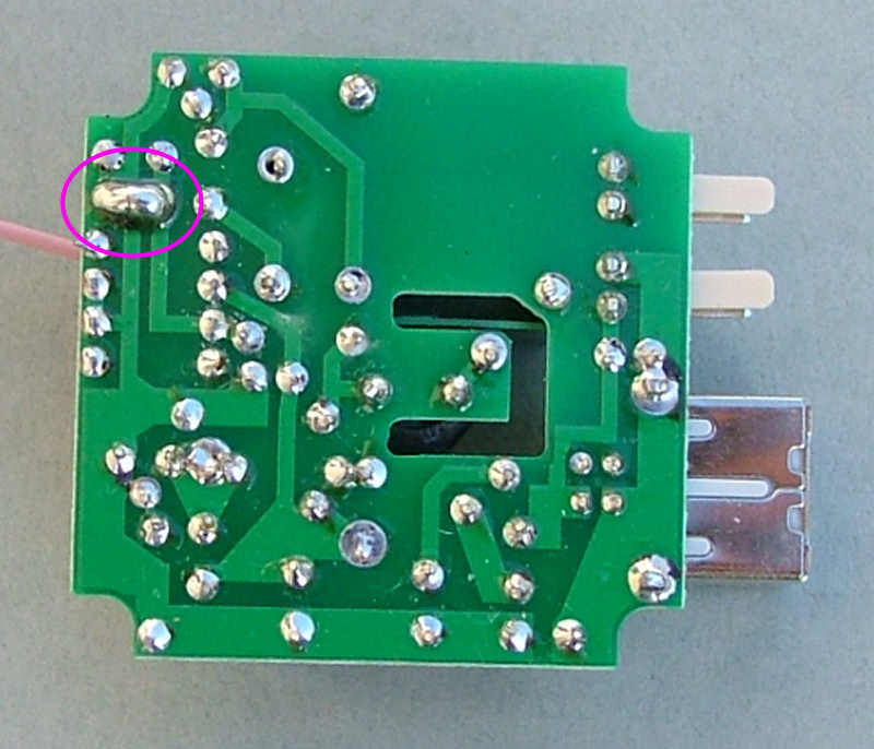
Solder the 2 tails to the pads shown, one between C1/C2 and the other next to T1:

Re: PCB assembly
Posted: Sun Apr 19, 2015 5:45 pm
by Tony
Almost time to power it up for the first time. Before that though, bridge the 2 pins of C6 or R4 to prevent damage to the PIC if anything goes wrong:

Re: PCB assembly
Posted: Sun Apr 19, 2015 5:47 pm
by Tony
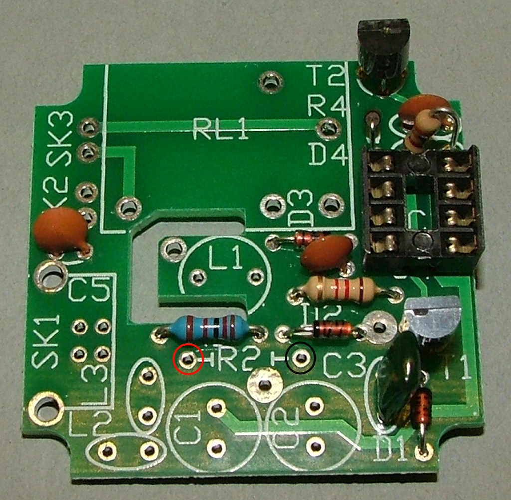
After making sure you have everything assembled correctly and the are no unwanted solder bridges fit IC1 into its' socket then connect a meter on a 200mA range to the pads of R2 (shown here on a partly assembled board for clarity):

Connect the USB lead to SK1 and the power supply. Make sure the L1 transformer isn't near the PCB, switch on and check you have a reading of 120-140mA. If it's a long way from this switch off and check everything again.
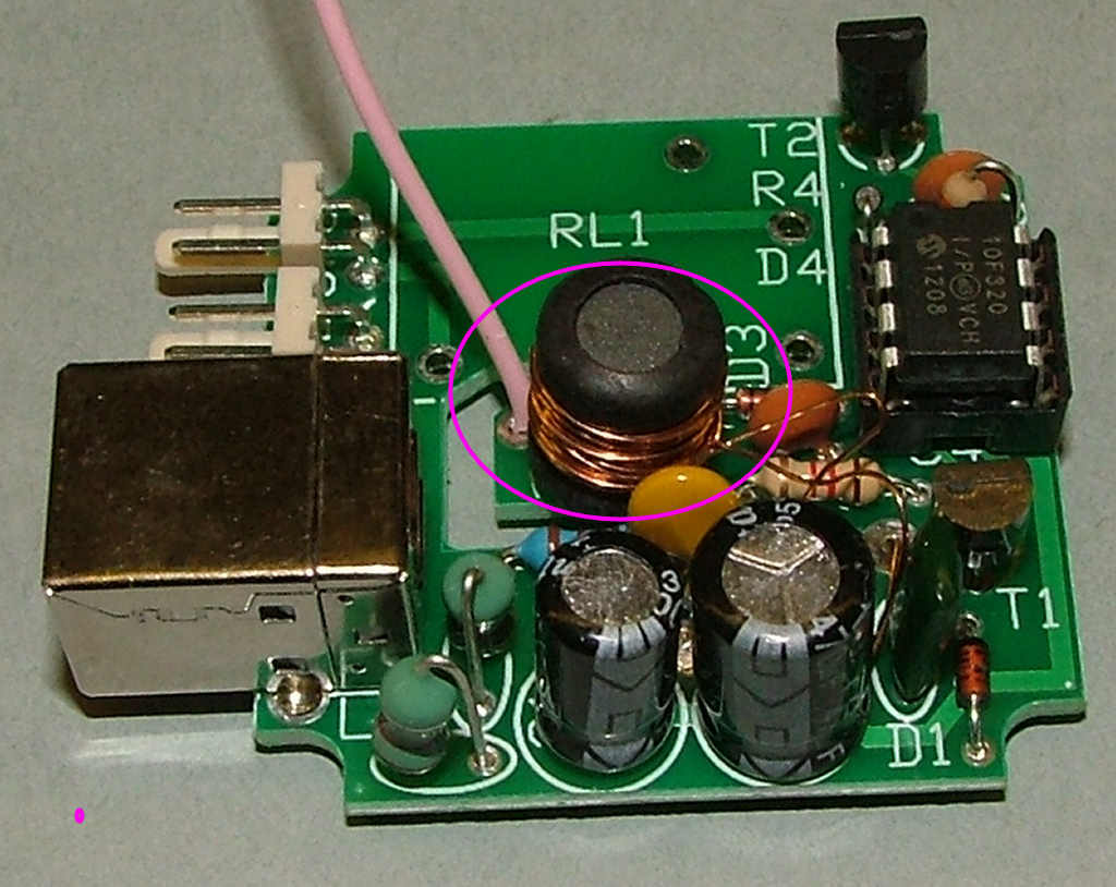
If the current reading is OK fit the coil assembly as shown. Strip and tin one end of the piece of insulated wire then connect the length of wire to the pad next to the transformer - this will connect to the nixie when the case is assembled.

Re: PCB assembly
Posted: Sun Apr 19, 2015 5:59 pm
by Tony
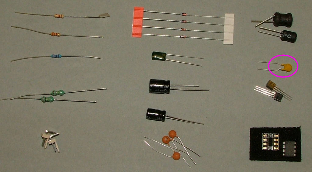
Fit R2 (Yellow resin bead) across the pads you used for the mA meter - this is a resettable fuse:

Re: PCB assembly
Posted: Sun Apr 19, 2015 6:03 pm
by Tony
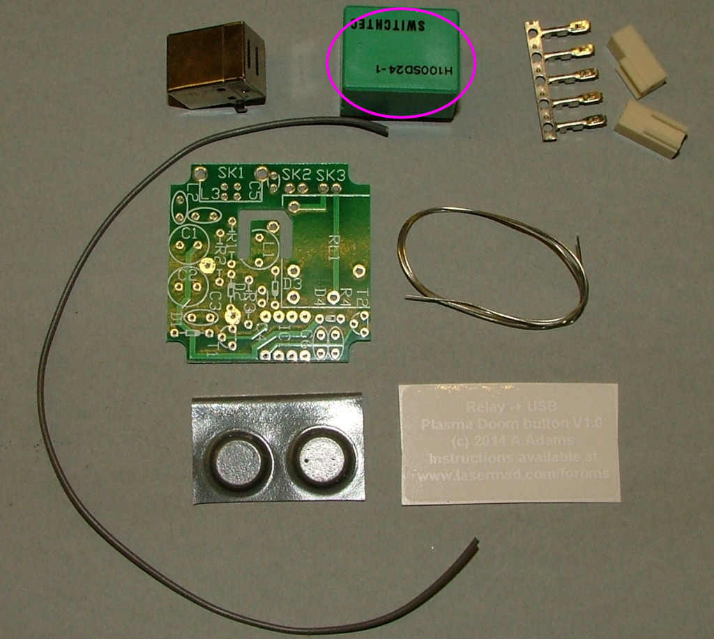
If you intend to use the relay now is the time to fit this, remeber to remove that solder bridge across C6 or it won't switch:

Note that from 2020 an alternative relay is supplied, the original relays are no longer available. If you received a black relay instead of green, follow these modifications:
1. Cut the corner pin (directly under the AC voltage and current rating markings) that has no corresponding PCB hole off.
2. Bend the centre pin on the opposite side flat so it sticks out from the side of the relay.
3. Fit the relay, bridging from the flattened centre pin to the pad next to D4.
4. You'll notice one pin is not connected - it's to the left of the marking for T2. Connect a short piece of wire from this pad to the cathode of D4 (the banded end).
This will work as a momentary open relay. There is also little clearance between the relay body and the 2-pin connectors so smaller 90 degree headers are now used.
